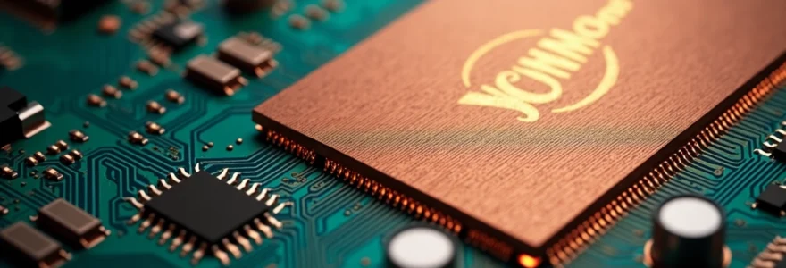
Heavy copper PCBs have become increasingly popular in high-power electronic applications due to their unique properties and performance advantages. These specialized printed circuit boards utilize copper layers with significantly greater thickness than standard PCBs, typically ranging from 3 oz/ft² (105 µm) to over 20 oz/ft² (700 µm). This increased copper weight offers a multitude of benefits that can greatly enhance the capabilities and reliability of electronic systems.
As power requirements for modern electronics continue to rise, heavy copper PCBs provide an effective solution for managing high currents, thermal loads, and mechanical stresses. From industrial power supplies to automotive systems and telecommunications infrastructure, these robust circuit boards are enabling engineers to push the boundaries of what’s possible in electronic design.
Thermal management enhancements in heavy copper PCBs
One of the primary advantages of heavy copper PCBs is their superior thermal management capabilities. The increased copper thickness allows for significantly improved heat dissipation compared to standard PCBs. This enhanced thermal performance is critical in high-power applications where excessive heat can lead to component failure and reduced system reliability.
Heavy copper layers act as efficient heat spreaders, rapidly conducting thermal energy away from hot spots on the board. This helps to distribute heat more evenly across the PCB surface, reducing the risk of localized overheating. Additionally, the larger cross-sectional area of heavy copper traces allows them to carry higher currents without experiencing as much resistive heating.
For applications requiring even greater thermal management, heavy copper PCBs can be combined with other cooling techniques such as thermal vias, heat sinks, or liquid cooling systems. The robust nature of heavy copper layers makes them well-suited for integration with these advanced thermal solutions.
Electrical performance improvements with increased copper weight
Beyond thermal benefits, heavy copper PCBs offer significant improvements in electrical performance across various parameters. These enhancements make them particularly valuable in high-power and high-frequency applications where signal integrity and power efficiency are paramount.
Reduced resistance and power loss in High-Current applications
One of the most notable electrical advantages of heavy copper PCBs is their reduced resistance in high-current paths. The larger cross-sectional area of heavy copper traces results in lower DC resistance compared to thinner copper layers. This reduction in resistance translates directly to decreased power losses and improved overall system efficiency.
For example, in a power supply design, using heavy copper for high-current paths can significantly reduce voltage drops and minimize wasted energy in the form of heat. This not only improves the power supply’s efficiency but also reduces the thermal load on other components, potentially extending the lifespan of the entire system.
Enhanced current carrying capacity and ampacity ratings
Heavy copper PCBs excel in applications requiring high current-carrying capacity. The increased copper thickness allows traces to handle much higher amperage levels without overheating or risking damage to the board. This enhanced ampacity is particularly valuable in power distribution systems, motor controllers, and other high-current electronic devices.
Engineers can take advantage of this increased current-carrying capacity to design more compact and efficient circuits. By using heavy copper layers, it’s possible to reduce the width of high-current traces while still meeting ampacity requirements. This can lead to significant space savings and potentially reduced overall board size.
Impedance control for RF and High-Speed digital circuits
While often associated with high-power applications, heavy copper PCBs also offer benefits for high-frequency and high-speed digital circuits. The increased copper thickness can provide better control over trace impedance, which is crucial for maintaining signal integrity in these demanding applications.
In RF circuits, heavy copper layers can be used to create low-loss transmission lines with precise impedance characteristics. This can lead to improved performance in applications such as antenna feed networks, power amplifiers, and microwave circuits. For high-speed digital designs, heavy copper can help maintain consistent impedance along critical signal paths, reducing reflections and improving overall signal quality.
EMI shielding effectiveness in noisy environments
Heavy copper layers can significantly enhance the electromagnetic interference (EMI) shielding capabilities of a PCB. The increased thickness provides better attenuation of electromagnetic fields, helping to protect sensitive circuits from external noise sources and preventing interference between different sections of a complex system.
This improved EMI shielding is particularly valuable in applications where electronic devices must operate in close proximity to other equipment or in environments with high levels of electromagnetic noise. Industries such as automotive, aerospace, and industrial automation can benefit greatly from the enhanced EMI protection offered by heavy copper PCBs.
Mechanical strength and durability advantages
Beyond electrical and thermal benefits, heavy copper PCBs offer substantial improvements in mechanical strength and durability. These properties make them well-suited for applications in harsh environments or those subject to physical stress.
Increased flexural rigidity and dimensional stability
The added copper weight in heavy copper PCBs contributes significantly to the overall rigidity of the board. This increased stiffness helps maintain the PCB’s shape and prevents warping or flexing under thermal or mechanical stress. For large boards or those subjected to vibration, this enhanced rigidity can be crucial in preventing solder joint failures and maintaining long-term reliability.
Additionally, the increased copper thickness can improve the dimensional stability of the PCB across temperature fluctuations. This is particularly important for applications where precise component alignment must be maintained over a wide operating temperature range.
Improved plated Through-Hole (PTH) reliability
Heavy copper PCBs offer significant advantages when it comes to plated through-hole (PTH) reliability. The thicker copper plating in the holes provides better mechanical strength and improved current-carrying capacity. This is especially beneficial for high-power applications where PTHs may be required to handle substantial currents.
The increased copper thickness in PTHs also enhances their ability to withstand thermal cycling without developing cracks or failures. This improved reliability is critical for applications in automotive, aerospace, and industrial environments where PCBs may be subjected to extreme temperature variations and thermal shock.
Enhanced vibration and shock resistance
The robust nature of heavy copper PCBs makes them highly resistant to damage from vibration and mechanical shock. The increased copper thickness provides better support for components and helps distribute mechanical stresses more evenly across the board. This enhanced durability is particularly valuable in applications such as automotive electronics, industrial machinery, and military equipment where PCBs may be subjected to harsh operating conditions.
Furthermore, the improved mechanical strength of heavy copper layers can reduce the risk of trace cracking or separation under repeated stress or impact. This contributes to the overall longevity and reliability of the electronic system in demanding environments.
Design considerations for heavy copper PCBs
While heavy copper PCBs offer numerous benefits, their design and fabrication require special considerations to fully leverage their advantages. Engineers must carefully balance the electrical, thermal, and mechanical requirements of their application when incorporating heavy copper layers into their PCB designs.
One key consideration is the impact of increased copper thickness on overall board thickness and weight. Heavy copper layers can significantly increase the total PCB thickness, which may affect packaging constraints or thermal management strategies. Designers must also account for the different etching and plating requirements of heavy copper, which can impact minimum trace widths and spacing.
Another important factor is the potential for increased manufacturing costs associated with heavy copper PCBs. The specialized processes required for fabricating these boards can result in higher production expenses compared to standard PCBs. However, for many high-power or high-reliability applications, the performance benefits and long-term reliability improvements often justify the additional cost.
When designing with heavy copper, it’s crucial to work closely with PCB manufacturers experienced in heavy copper fabrication. These specialists can provide valuable guidance on design rules, manufacturing limitations, and best practices for optimizing heavy copper PCB designs. As noted by icape-group.com, partnering with experienced fabricators is essential for successful heavy copper PCB implementation.
Manufacturing processes specific to heavy copper layers
The fabrication of heavy copper PCBs involves several specialized manufacturing processes that differ from those used for standard PCBs. These techniques are crucial for achieving the desired copper thickness while maintaining precise dimensional control and ensuring the integrity of the final product.
Advanced etching techniques for thick copper foils
Etching heavy copper layers requires advanced techniques to achieve clean, well-defined traces without undercutting. Traditional etching methods can lead to excessive lateral etching, resulting in trapezoidal trace profiles that may compromise signal integrity or current-carrying capacity.
To address this challenge, manufacturers employ specialized etching processes such as differential etching or step etching. These techniques involve multiple etching stages with varying chemical concentrations and exposure times to achieve more vertical sidewalls on copper traces. This results in more precise trace geometries and better overall performance in the final PCB.
Plating methods for uniform copper distribution
Achieving uniform copper thickness across the entire PCB surface is critical for heavy copper designs. Standard plating processes may result in uneven copper distribution, with thicker deposits on outer layers and thinner plating in high-aspect-ratio holes.
To overcome this challenge, manufacturers use advanced plating techniques such as pulse plating or reverse pulse plating. These methods provide better control over the plating process, resulting in more uniform copper deposition across all board features. This uniformity is essential for maintaining consistent electrical and thermal performance throughout the PCB.
Specialized drilling and via formation procedures
The increased copper thickness in heavy copper PCBs necessitates specialized drilling and via formation procedures. Standard drilling techniques may struggle to produce clean, precise holes through thick copper layers without causing burrs or smearing.
To address this, manufacturers often employ high-speed spindles, specialized drill bits, and optimized drilling parameters. For very thick copper layers, techniques such as controlled depth drilling or back drilling may be used to achieve the desired hole quality.
Via formation in heavy copper PCBs also requires careful consideration. The increased aspect ratio of vias in thick boards can make it challenging to achieve uniform plating and reliable connections. Manufacturers may use advanced via filling techniques or stacked micro-vias to ensure robust interconnections between layers.
Cost-effectiveness and Long-Term reliability analysis
While heavy copper PCBs typically have higher upfront manufacturing costs compared to standard PCBs, they can often prove more cost-effective in the long run for certain applications. The improved reliability, enhanced performance, and potential for design simplification can lead to significant savings over the lifecycle of a product.
For high-power applications, the use of heavy copper can eliminate the need for additional components such as bus bars or power planes, potentially reducing overall system complexity and cost. The improved thermal management capabilities may also reduce or eliminate the need for expensive cooling solutions in some designs.
From a reliability standpoint, heavy copper PCBs often demonstrate superior longevity in demanding applications. The reduced risk of thermal damage, improved resistance to mechanical stress, and enhanced EMI shielding can all contribute to fewer field failures and extended product lifespans. This increased reliability can lead to substantial cost savings in terms of reduced warranty claims and maintenance requirements.
When evaluating the cost-effectiveness of heavy copper PCBs, it’s essential to consider the entire system lifecycle, including factors such as:
- Initial manufacturing costs
- Potential reductions in component count or complexity
- Improved energy efficiency and operating costs
- Reduced maintenance and repair expenses
- Extended product lifespan
By carefully analyzing these factors in the context of specific application requirements, engineers can make informed decisions about when and where to implement heavy copper PCB technology for maximum benefit and cost-effectiveness.